Researchers at the University of Minnesota Twin Cities have unveiled the Computational Random-Access Memory (CRAM) hardware architecture, poised to transform AI computing by drastically reducing energy consumption. CRAM promises to cut energy use for AI applications by a factor of 1,000, addressing a major challenge in the field.
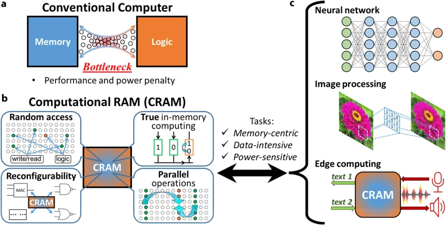
CRAM, or Computational Random-Access Memory, is a hardware technology developed to address the high energy demands of AI computing. Unlike traditional architectures, CRAM processes data directly within memory cells, eliminating the need for energy-intensive data transfers between logic units and memory. This innovation drastically improves energy efficiency, offering potential energy savings of up to 1,000 times compared to conventional methods. CRAM’s unique design allows for in-memory computation, random access, reconfigurability, and parallel operations, making it ideal for data-intensive and power-sensitive applications such as neural networks and image processing.

Energy Consumption Problem in AI
The International Energy Agency (IEA) projects AI energy consumption to more than double, from 460 terawatt-hours (TWh) in 2022 to 1,000 TWh by 2026, equivalent to Japan’s total electricity usage. Traditional AI computation involves energy-intensive data transfers between logic units and memory. CRAM eliminates this by processing data entirely within the memory array.
A Shift from Traditional Architecture
CRAM signifies a fundamental departure from the traditional von Neumann architecture, which has been the backbone of modern computers. By enabling computation directly within memory cells, CRAM eliminates the computation-memory bottleneck. Ulya Karpuzcu, an Associate Professor in the Department of Electrical and Computer Engineering and co-author of the paper, highlighted CRAM’s flexibility in reconfiguring to match the performance needs of diverse AI algorithms.
The technology leverages spintronic devices that use the spin of electrons to store data, offering significant advantages over traditional transistor-based chips, including higher speed, lower energy consumption, and resilience to harsh environments.
The CRAM-based machine learning accelerator could achieve energy savings up to 2,500 times compared to conventional methods. This breakthrough is the culmination of over 20 years of research led by Jian-Ping Wang, a Distinguished McKnight Professor and Robert F. Hartmann Chair in the Department of Electrical and Computer Engineering.
Evolution of CRAM Technology
Wang reflected on the initial concept of using memory cells directly for computing, considered “crazy” two decades ago. An interdisciplinary effort involving students and faculty from various fields, including physics, materials science, engineering, computer science, and hardware creation, led to the development of this feasible technology.
The CRAM architecture builds on the team’s earlier work with Magnetic Tunnel Junctions (MTJs) and nanostructured devices. These components, already used in hard drives and sensors, form the basis of Magnetic Random Access Memory (MRAM), implemented in microcontrollers and smartwatches.
Experimental Results and Future Prospects
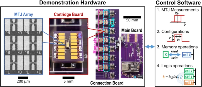
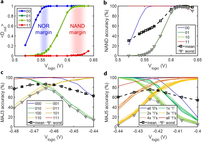
The team conducted extensive experiments demonstrating CRAM’s capabilities. They achieved reliable memory write operations with an average write error rate of less than 1.5 × 10^-4. The device demonstrated high accuracy in logic operations, with a 2-input NAND operation showing an accuracy of about 99.4%.
With multiple patents secured, the research team aims to collaborate with semiconductor industry leaders to scale up their demonstrations and produce hardware that can advance AI functionality. Details of the team’s research were published in the peer-reviewed journal npj Unconventional Computing.
This innovation not only promises to make AI more energy-efficient but also reimagines the future of AI computing with its flexible, efficient, and sustainable architecture.
